Application Specific Integrated Circuit
What is ASIC?
Application specific integrated circuits are highly specialized devices. Unlike other devices, ASICs are non- standard integrated circuits constructed for one specific purpose application only. The work related to ASIC began in the early 1980s itself. Today, we can see that Application Specific Integrated Circuit (ASIC) are changing the way electronic device systems are designed, manufactured, and marketed. So, it is important in this challenging design world to understand the nature, options, design methodologies, and costs of ASIC technology. Some examples of ASIC chip include chips for satellites, chips designed to run a cell phone, Bitcoin Miner, chip used in a voice recorder etc. Some ICs that are not ASICs include memory chips like ROM, DRAM; ICs at LSI, SSI and MSI levels etc.
Using an ASIC chip, the major advantage is that, overall design can be made into one integrated circuit and the number of additional circuits can be reduced. Modern ASIC chip designs generally include 32-bit processors, memory blocks and other large building blocks. Such a modern ASIC chip is known as SoC (System-on-a-Chip). Usually, ASIC designs will be carried out only for those products which have large production run. Also, since the cost of ASIC chip is high, it is recommended only for high volume products. Today, many digital ASIC designers use hardware description languages (HDLs) like Verilog and VHDL, to describe the function and design of ASIC chip.
Types of ASIC
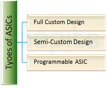
There are basically three types of ASIC chip designs: Full Custom Design, Semi-Custom Design and Programmable ASIC.
 Full Custom Design
Full custom Design is a design methodology useful for integrated circuits. In this design, the resistors, transistors, digital logic, capacitors and analog circuits are all positioned in the circuit layout. Generally full custom designs are referred as “handcrafted” designs.Microprocessor is a simple example of full custom IC. Usually; the manufacturing and design of it is very expensive. 8 weeks is the normal manufacturing lead time.
Maximum performance, minimized area and highest degree of flexibility are the major features of this design. While; the risks of such an IC is higher because the whole design is untested and not designed from the library elements that have been used before. Also, it requires designers that are highly skilled and may take many years to finish the design. Full Custom ICs also helps to concentrate an intended specific design application mainly.
Semi- Custom Design
Semi-Custom design is an alternative to full-custom designs. Here, we can use components from a standard library for design purposes. Thus, in semicustom ASIC designs, all logic cells are predesigned and some mask layers are only customized. The advantage of using predesigned logic cells from the library is that, it can make semi-custom ASIC chip designs easier. Standard cell libraries are usually designed using full custom designs. There are basically two types of semicustom ASICs: Standard Cell Based ASIC and Gate Array Based ASIC.
Standard Cell Based ASICs
A standard cell based ASIC commonly uses predesigned logic cells like logic gates, flip flops, multiplexers, demultiplexers etc. These predesigned logic cells are known as Standard Cells. Flexible blocks also known as standard cell areas in the ASIC design consist of many rows of standard cells. The standard cell areas can be usually used in combination with larger standard cells like microcontrollers. The larger standard cells are also known by the names Megacells, Megafunctions, System Level Macros, Full custom blocks, Fixed Blocks, cores or System Level Macros.


Placement and providing Interconnection of cells is the major role of the ASIC designer here. Some advantagesof using standard cell based designs include save money, reduced time and less risk compared to full custom designs. The disadvantage is the time and expense to make a standard library and to fabricate these designs.
Table 1: Examples of Standard Cell Products

Gate Array Based ASIC
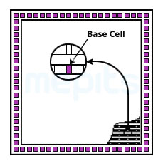
Gate Array Based ASIC chip is a prefabricated silicon chip in which transistors, logic gates, and other active devices are placed at predefined positions and manufactured on a wafer. Predefined pattern of gate array based ASIC is known as Base Array. The element or logic cell present in the base array is often called asBase Cell. Usually gate array based ASIC designs are known popularly by the name Masked Gate Array. Here the ASIC designer can choose predesigned logic cells from the gate array library for better and easy design. The cells present in the gate array library are often called as Macros. Reduced time, low cost are some of its advantages compared to standard cell and full custom designs.
Table 2: Examples of Gate Array Products


Three types of Gate Array Based ASICs are: Channeled Gate Arrays, Channeless Gate Arrays and Structured Gate Array. In Channeled Gate Array, the space for interconnect between the rows of cells are fixed in height. While in Channeless Gate Array, there is no predefining space between the rows of cells. Structured Gate Array or Embedded Gate Array combines both the features of standard cell based and gate array based ASICs.


Figure: Channeless Gate Array and Structured Gate Array
Programmable ASIC
Programmable ASICs are classified into Programmable Logic Devices and Field Programmable Gate Arrays.
Programmable Logic Devices (PLDs)
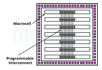
PLDs are electronic devices used to build reconfigurable circuits. Unique features of PLDs are fast turn around, large programmable interconnect, no customized logic cells and mask layers. PAL, PLA, GAL ROM, PROM, EPROM, EEPROM, UVPROM etc. are some examples of programmable ICs.
Table 3: Examples of some PLD Products


Field Programmable Gate Arrays (FPGAs)
FPGAs are complex and larger reconfigurable devices. Unique features of Field Programmable Gate Arraysinclude programming logic cells and interconnect and here no mask layer is customized. Xilinx, Altera, QuikLogic, Actel etc. are some of the important FPGA companies.
Table 4: Examples of FPGA

ASIC Design
There are various steps involved in the ASIC chip design. A brief description is given below.

- Design Entry: In this step, the designer starts the design with a text description or system specific language like HDL, C language etc.
- Logic Synthesis: Logic synthesis generally helps to produce the netlist consisting the description and interconnection of logic cells.
- System Partitioning: Here partitioning of a large design into a small ASIC design takes place.
- Prelayout Simulation: Prelayout Simulation allows checking whether the design functions correctly.
- Floorplanning: Using this step we can plan the arrangement of the blocks present in the netlist on the chip
Asics video how it works
No comments:
Post a Comment